Ideas & Solutions
The plated through hole calculation
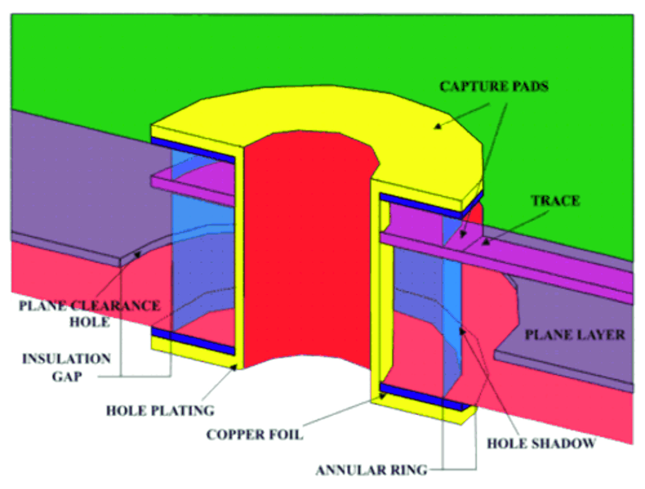
A clear understanding of the anatomy of a plated through hole (please see the picture below) is necessary in order to satisfy the dual needs of assembly and PCB fabrication. The PCB assembler works with finished hole size. The fabrication process is based on the drilled hole size.
 Along with all of this, it is necessary to size holes in such a way that the power planes of the PCB are not degraded by placing holes so close together that they cause slots to be created in the planes by overlapping clearance holes. It is not possible to specify generously large hole sizes and insulation spacing to make manufacturing or fabrication easy without risking degradation of the environment needed by the high speed signals travelling across those planes through the PCB. Also see the critical values of "Copper trace/pad to drill hole" and "Min pad over drill size" in "PCB capabilities" table.
More details how correctly to calculate the sizes of pads and keep out areas needed to insure the PCB you can find in article of Lee W. Ritchey here.
Along with all of this, it is necessary to size holes in such a way that the power planes of the PCB are not degraded by placing holes so close together that they cause slots to be created in the planes by overlapping clearance holes. It is not possible to specify generously large hole sizes and insulation spacing to make manufacturing or fabrication easy without risking degradation of the environment needed by the high speed signals travelling across those planes through the PCB. Also see the critical values of "Copper trace/pad to drill hole" and "Min pad over drill size" in "PCB capabilities" table.
More details how correctly to calculate the sizes of pads and keep out areas needed to insure the PCB you can find in article of Lee W. Ritchey here.
Hide topics
